Advances in beam delivery
enable high-precision manufacturing
|
Today, ultrafast lasers (ultrafast-pulsed lasers with pulse durations in
the femtosecond and picosecond range) are an important part of many
industrial processes. The ability of these lasers for high-quality,
virtually athermal material processing, coupled with advances in laser
technology, process development, beam handling, and delivery, have opened
the door for numerous advanced scientific and industrial applications.
However, to achieve economic break-even points, several criteria must be
simultaneously fulfilled. First, the technical feasibility of the
industrial process has to be demonstrated. Because of the unique nature
of ultrafast laser-matter interaction, this usually requires a
sophisticated scientific understanding of the process. Second, the productivity
of the industrial process must guarantee a sufficient return on
investment for the end user. This has led to an important effort in laser
development towards high-average-power ultrafast lasers, which in turn
requires advances in beam handling and delivery to take full advantage of
the potential processing speed. Nowhere else than in consumer electronics
applications are these trends more in evidence. Cell phones,
microprocessors, display panels, and memory chips are extremely
sophisticated components, comprising a large number of different
materials, multiple layers of extremely low thicknesses, and very small
features. They require advanced and high-precision manufacturing
processes, as well as the capability to be produced economically in large
quantities. The following examples will outline the need for simultaneous
development of process understanding, laser technology, and new beam
delivery technique to meet present and future challenges. FIGURE 1.
Thin-film transistor electrode cutting, with cut width of 1.9μm.
(Courtesy: Korean Institute of Metals and Machinery) Manufacturing
flat-panel displays for cell phones, tablets, or TVs is one of the most
complex technological endeavors today-on par with the Apollo program
development in the 1960s or arguably even more difficult. The different
production steps involve a number of different materials, with micrometer
lateral resolution and layers a few 10s of nanometers thick. Given the
difficulty of the entire process, it is no surprise that the industrial
yield (the percentage of units that pass the stringent quality control)
is both a closely guarded secret and a major challenge. A key limitation
is the presence on a panel of a few "dead" pixels, which will
prevent the commercialization of the screen. For the past several years,
different repair
|
|
FIGURE 1. Thin-film transistor electrode cutting, with cut width
of 1.9μm. (Courtesy: Korean Institute of Metals and Machinery)
|
|
processes-usually
involving multi-wavelength nanosecond lasers-have been developed. For
instance, a bright pixel might be destroyed, either by laser
carbonization or by cutting the electrode of the thin-film transistor
controlling the pixel (FIGURE 1).
|
|
Today, current techniques are reaching their limits. Because of the
improvement in the resolution of high-definition screens, the pixel size
is becoming smaller and thermal effects associated with nanosecond laser
processing are limiting the quality of the repair. Moreover, new display
technologies, such as organic LEDs (OLEDs) and active-matrix OLEDs
(AMOLEDs), make extensive use of organic and polymer materials, which are
highly sensitive to heating and incompatible with thermal processing.
Because of their very short pulse duration, ultrafast lasers allow for
virtually athermal micromachining without any heat generation. Their
increasing use in the advanced display repair process led to the
development of a new generation of compact, high-speed, multi-wavelength
ultrafast lasers. Several industrial processes have been developed to
take advantage of the high precision of ultrafast laser processing. This
includes selective layer ablation, where ablation rates as precise as
30nm per pulse are routinely achieved, and high-precision thin-film
transistor electrode cutting, which has a cutting width smaller than 2μm.
These processes require the development of advanced and flexible beam
shaping techniques, allowing the delivery of uniform, flat-top beams with
variable shape to the sample and sizes as low as 2 × 2μm. In another
example, semiconductor circuits are becoming increasingly sophisticated.
They integrate more functions, with smaller feature sizes. To this end,
wafers are now comprised of many layers of multiple materials, such as
low-k materials for faster operation. An important process in
semiconductor manufacturing is the wafer dicing-or singulation-step,
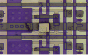
where a wafer is cut into individual dies (FIGURE 2).
Traditionally done with diamond saws, current techniques are now reaching
their limitation. Due to low-k materials' brittleness, lower thickness,
and high number of layers, adverse effects such as cracks and
delamination are increasingly liable to occur.
|
|
FIGURE 2. Semiconductor wafer dicing and scribing. (Courtesy:
Amplitude Systemes)
|
|
|
Although there is a
strong development drive using ultraviolet (UV) nanosecond lasers, the
thermal effects associated with nanosecond laser processing represent a
strong limitation in the quality of the results. On the other hand,
ultrafast lasers have demonstrated their capability to process silicon
and multiple materials with a high quality. Until recently, a main
limitation was the limited average power available from ultrafast lasers,
which severely limited the overall throughput. The recent development of
industry-ready, high-reliability femtosecond lasers in the 50-100W range
allows reaching throughput compatible with industry requirements.
Ultrafast lasers are an essential part of many advanced micromachining
processes, and they also play a significant role in quality control and
metrology. Rudolph Technologies (Flanders, NJ; www.rudolphtech.com) recently
introduced a new industrial tool for the measurement of opaque thin-film
thickness in the semiconductor industry. The system is based on acoustic
wave measurement and uses a very short, laser-generated ultrasound pulse.
The timing of the reflections of this ultrasound pulse on the various
layer interfaces is measured using a pump-probe technique with high
accuracy.
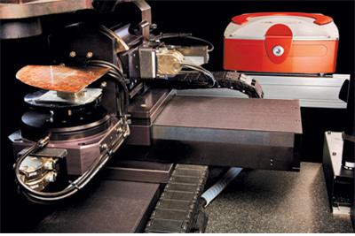
In another example, CAMECA (Gennevilliers, France; www.cameca.com) is able to perform 3D
imaging and analytical characterization of semiconductor and metal
samples, with atom-scale resolution. This incredible measurement process
is based on a technique called atom-probe tomography, which involves
irradiating a nanometer-radius tip of a sample with an ultrafast laser (FIGURE 3).
If the power of the laser is carefully controlled, instead of laser
ablation, a gentle atom-by-atom evaporation takes place. Each atom is
then sent onto a position-sensitive detector, which determines the
location on the tip from which it comes. In addition, a time-of-flight
mass spectrometer measures the atomic weight and, therefore, the tip
composition. Then, 3D reconstruction is performed layer by layer. This
method is used in the semiconductor industry to monitor the composition
and impurities of the semiconductor material, as well as in metallurgy to
control, at a very fine scale, the quality of metallurgical alloys.
|
|
Manufacturing and quality
control benefit from the increasing availability of high-power,
|
|
FIGURE 3. The atom-probe tomography principle.(Courtesy: CAMECA)
|
|
high-reliability laser
systems. More specifically, ultrafast lasers with average power in the
range of 50 to 200W increase throughput and productivity, and, in a
virtuous circle, allow the development of new applications. And yet, beam
handling and delivery of such high-power lasers is not straightforward.
Processing speeds of up to 100 m/s are required to reach economic
break-even while maintaining micrometer-scale positioning accuracy. And
the current generation of galvanometric mirror-based scanners is reaching
its limit, calling for new approaches.
ESI (Portland, OR; www.esi.com) has
introduced a hybrid processing system that combines galvanometer mirrors
and acousto-optic technology. When operating at a high processing speed,
the inertia of the scanner mirrors means that they will lag somewhat when
performing, for instance, a sharp turn, so the processed structure will
not have the desired shape. Acousto-optic modulators, however, exhibit
extremely high reactivity, but on a very small field. The combination of
mirror movement and acousto-optic deflection, precisely synchronized,
overcomes this limitation. Such a technique is especially useful in the
manufacturing of interconnected digital circuit patterns, which are
becoming more tightly integrated and require increased wiring density.
Researchers at DISCO (Tokyo, Japan; www.disco.co.jp)
have combined the two approaches by simultaneously performing
micromachining and process control with the same laser. The application
in this case is blind via-hole drilling of a two-layer substrate with an
ultrafast laser. The upper layer is a transparent material with a
thickness of 80μm and the lower layer is a 20μm-thick metal film. To
precisely control the number of laser pulses required to achieve ablation
of the transparent substrate only, the plasma emission is monitored with
an optical spectrum analyzer using a technique known as laser-induced
breakdown spectroscopy (LIBS). Since the plasma emission has a unique
emission spectrum depending on the atomic species being ablated, it is
possible to clearly and accurately identify the instant when the
transparent layer is fully ablated.
In another approach, polygon scanners can provide scanning speeds greater
than 100 m/s. Instead of using low-inertia galvanometer mirrors to
deflect the beam in the x and y directions, a single, multifaceted
polygonal mirror rotates at a high speed. If the pulse laser is precisely
synchronized with the polygonal mirror rotation, only a single spot per
facet may impact the sample to be processed. In this case, the
micromachining process is closer to a digital process, where the laser
has to be switched on and off to produce the desired pattern. To be
successful, though, this approach requires very precise synchronization
between the laser and the scanner, high manufacturing accuracy of the
polygonal mirror, as well as a carefully designed process. Prof. Beat
Neuenschwander (Bern University of Applied Sciences,
Switzerland; www.bfh.ch), in
collaboration with Amplitude Systèmes and NextScan (Evergem, Belgium; www.nextscantechnology.com),
has demonstrated high-speed surface texturing with a 500kHz ultrafast
laser and micrometer-scale repositioning accuracy. Still, more innovative
beam delivery approaches are on the way. Industrial ultrafast lasers,
until recently, were not able to benefit from fiber-optic delivery
systems, which have transformed laser manufacturing. The confinement of
the beam in a small fiber core, combined with the very high peak
intensity associated with ultrafast pulses, gave rise to severe nonlinear
effects and ultimately fiber degradation. To mitigate this limitation,
microstructured fibers with hollow cores have been developed, but their
core diameter is limited to a few microns-too small for practical use.
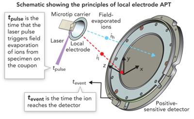
The development of hollow-core, large-mode-area Kagome microstructured
fibers paves the way for fiber delivery of high-energy, high-power
femtosecond laser beams. The special, hypocycloidal shape of the hollow
fiber core confines the laser mode, prevents it from interacting with the
fiber microstructure, and provides a combination of low nonlinearity,
large mode area, and flexible dispersion control. In collaboration with
the company Glo Photonics (Limoges, France; www.glophotonics.fr), Amplitude
Systèmes has demonstrated the delivery of millijoule-class pulses over a
distance of several meters, while maintaining a sub-500fs pulse duration.
In another set of experiments, performed in a collaboration with the
company Photonics Tools (Berlin, Germany; www.photonic-tools.de), average
power of 100W has been transmitted and pulse compression to sub-100fs
pulses has also been demonstrated. Other teams and laser manufacturers
are quickly refining and developing flexible delivery systems using
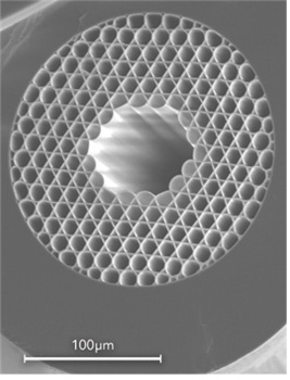
Kagome fibers (FIGURE 4), and we can expect a
profound transformation of ultrafast laser processing systems in the
years to come.
Enabled by advances in the physics of short-pulse laser-matter
interaction, as well as technological developments in beam handling and
delivery systems, ultrafast lasers have made
|
|
FIGURE
4.A Kagome fiber's core
shape. (Courtesy: CNRS/Glo Photonics)
|
|
their way into the heart
of our daily lives. Deeply embedded into the most advanced industrial
manufacturing processes, they are changing the way we see, the way we
communicate, and the way we work, and are a key of future generations of
consumer electronic devices of increased complexity.
|
|
원문정보 : http://www.industrial-lasers.com/articles/print/volume-30/issue-2/features/ultrafast-
lasers-for-consumer-electronics.html
|
|
|